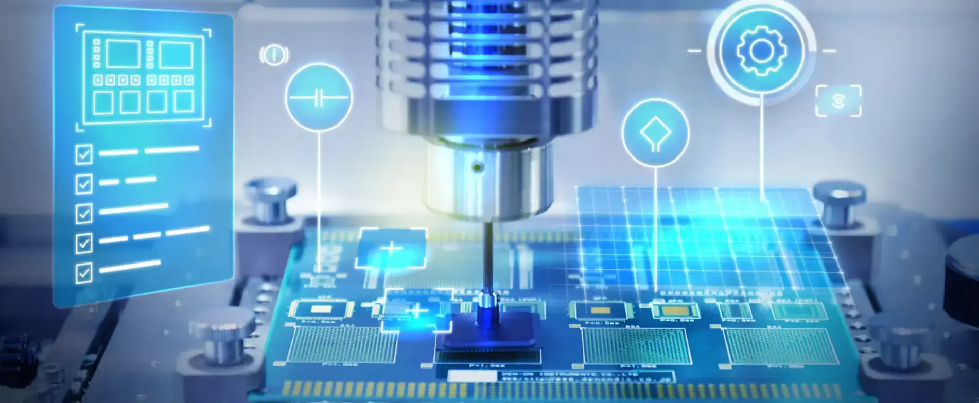
AI-Driven Inspection for Advanced Process Nodes
As semiconductor manufacturing advances toward 7nm, 5nm, and even 2nm process nodes, defect inspection faces unprecedented technical challenges. Wafer surface defects are becoming smaller, less visible, and more complex in morphology. Traditional approaches based on rule-based image comparison and manual review increasingly encounter limitations in accuracy, throughput, and scalability.
AI-powered inspection systems have emerged as a key enabler for next-generation yield management. With high-performance AI servers at the core, image recognition, model training, and data orchestration tasks can be executed efficiently—transforming inspection workflows from experience-driven processes to compute-centric, automated systems.

Beyond GPUs: The Critical Role of CPU–GPU Collaboration
AI workloads are often associated primarily with GPUs. However, in high-precision, long-process, real-time semiconductor inspection environments, overall system performance depends on tight collaboration between GPU acceleration and CPU orchestration.
| Inspection Stage | Task Description | Primary Compute Dependency |
|---|---|---|
| Image Acquisition & Preprocessing | Image decoding, grayscale conversion, geometric correction, data consolidation | High-frequency CPU, multi-threaded parallel processing |
| Feature Extraction & Structural Analysis | Edge detection, region segmentation, anomaly localization | CPU with partial GPU acceleration |
| Deep Learning Inference | CNN and Transformer-based defect classification | GPU batch parallel processing |
| Multi-Model Fusion & Rule-Based Decision | Model ensemble, rule filtering, coordinate output | CPU serial decision logic and workflow control |
| Image Archiving & Data Return | File compression, data packaging, storage operations | CPU with high storage bandwidth support |
Within AI inspection pipelines:
- GPUsaccelerate deep learning inference and training.
- CPUsmanage data ingestion, logic control, multi-model integration, task scheduling, and I/O orchestration.
High-frequency, multi-threaded CPU performance is essential to ensure stable data feeding, deterministic execution, and real-time responsiveness across the inspection chain.
Core Scenario 1: High-Precision Defect Image Inference
Wafer fabrication and packaging stages generate terabytes of high-resolution image data daily. Inspection systems must deliver millisecond-level response times while maintaining sub-pixel detection accuracy.
Commonly deployed AI models include CNN-based architectures, Transformer-based vision models, and UNet-style segmentation networks, all of which demand strong parallel computing capabilities.
A multi-GPU AI server architecture enables:
- Micron-level defect detection (scratches, corrosion, particles, grain anomalies, etc.)
- Multi-model ensemble inference (classification, segmentation, detection fusion)
- Real-time automated labeling, binning, and feedback control
Meanwhile, high-clock CPUs handle front-end image decoding, geometric correction, and data preprocessing in real time, ensuring a continuous, optimized data pipeline for GPU inference workloads.
Core Scenario 2: Model Training and Continuous Optimization
Semiconductor defects are highly dynamic and non-structured. Static models quickly degrade in performance across process variations, tool changes, or batch differences. Continuous retraining and calibration are therefore essential.
AI servers provide the following capabilities for training environments:
- Multi-GPU parallel training with mixed precision (FP16) acceleration
- High-speed NVMe storage for rapid dataset loading
- CPU-managed task scheduling, parameter control, and validation workflows
In production environments, training pipelines are often integrated with manufacturing execution systems (MES), forming a closed-loop workflow:
Data Collection → Model Training → Deployment → Feedback → Retraining
This closed-loop architecture enables adaptive inspection systems capable of evolving alongside process changes.

Core Scenario 3: Data Acquisition and Archival Infrastructure
In automated inspection systems, image streams typically originate from high-speed industrial cameras (e.g., GigE, Camera Link, CoaXPress). After acquisition, the system must perform:
- Real-time decoding and parallel preprocessing (CPU memory bandwidth dependent)
- Result archival and sample annotation (disk I/O throughput dependent)
- Large-scale dataset classification and visualization (database and storage architecture dependent)
An AI server in this context functions not only as a compute engine, but also as a data hub. CPU memory bandwidth, storage array performance, and network throughput directly determine system stability, response latency, and scalability.

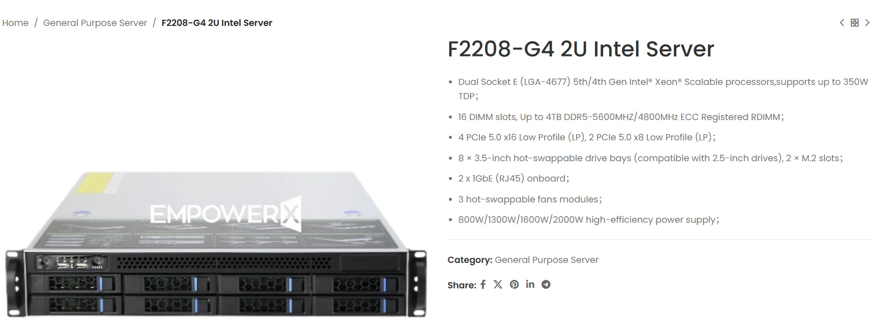
Recommended AI Server Configuration for Semiconductor Multi-Task Workloads
Module | Recommended Configuration | Technical Rationale |
|---|---|---|
| CPU | 2 × Intel Xeon Platinum 8558P or AMD EPYC 9654 | Supports sequential logic execution, task orchestration, and high-throughput I/O scheduling |
GPU | 1 × NVIDIA RTX 6000 Ada (48GB) | GPU acceleration for compute-intensive inference and model processing |
Memory | ≥ 512GB DDR5 ECC | Supports large-scale data buffering and model loading |
| storage | 2TB NVMe + 8TB Enterprise SSD, RAID 5 | High-speed read/write performance with secure data redundancy |
| Network | Dual 25GbE + IPMI Management | Enables multi-stream image transmission and remote monitoring/management |
| Form Factor | 2U Rackmount, cleanroom-compatible thermal design | Standardized rack integration for rapid deployment in production environments |
Conclusion: Compute as the Foundation of Intelligent Inspection
From defect image inference and model optimization to data acquisition and archival management, AI servers have evolved beyond simple accelerators. They now serve as the computational core of intelligent semiconductor inspection systems.
By combining high-performance CPUs, scalable GPU acceleration, and optimized storage and networking architectures, advanced AI infrastructure enables:
- Higher detection accuracy
- Lower latency response
- Continuous model evolution
- Greater production stability
As semiconductor manufacturing continues to scale in complexity, compute-centric architectures will remain fundamental to achieving automated, intelligent, and scalable inspection systems.
For detailed architecture documentation or technical whitepapers, please contact our engineering team for further information.